
Test wafer »
Product Range
We supply P-Type Test Wafer which is manufactured under show unparalleled outstanding performance by virtue of high density, excellent purity, and distinguished homogeneous microstructure. The popular geometries featuring with both planar and rotatable shapes, such as circular, rectangular, ring, tube, cylinder and conicity, are all available. If you have your own unique requirements about the sputtering targets, no matter in density, purity, homogeneity or in geometry, please let us know exactly what you need. We'll do our utmost to meet your requirements precisely.
| Sl. No | Specifications |
| 1 | Process: CZ |
| 2 | Wafer Type: P-Type Silicon |
| 3 | Dopant: Boron |
| 4 | Back Side Damage: No (see back-side surface criteria) |
| 5 | Laser Mark: Frontside Deepmark, depth 45 +/- 15 um, 12 characters, character 1~5 lot number, 6~8 serialization number, 9~10 vendor code, 11~12 check digit. Top of mark towards the edge of wafer, OCR font, single row dot matrix 5x9 or SEMI STANDARD M13- Soft |
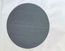
| 6 | Diameter: 200 (- 0.2/ +0.2 ) mm |
| 7 | Thickness: 725 ± 20 micron |
| 8 | Orientation - 1 Notch: D={110} +/- 1 deg as per Semi M1 STD |
| 9 | Bevel configuration: R = t/2t = 725 +/-20 micron |
| 10 | TTV : 50 micron (Max.) |
| 11 | Curvature (WARP) : 60 micron (Max) |
| 12 |
SFQR (TIR - Site) : 0.4 micron (max)SFQR = 0.4 um base on 95% PUA with a total of 60 sites & 16 partial sites. Site size = 22.5 x 22.5 mm with No offset. |
| 13 | TIR (PUA) - Site: 95% (with 3 mm edge exclusion) |
| 14 | Surface Impurities (x 10^10 atoms/cm2) : Na- 30, Al-500, Fe-50, Ni, Cr, Cu & Zn-10 MCL |
| 15 | Particles: 50 Counts of >=0.16 microns/wafer |
| 16 | Front Surface Finishing: Mirror Surface |
| 17 | Back Surface Finishing : Etched surface |
| 18 | Chip A: 2 (max) |
| 19 | Polished Surface Orientation. : 1-0-0+/- 1 degrees Resistivity : 0.5 to 1000 Ohm cm |
| 20 | Packing: SEP- A5 or Entegris Ultrapack |
Note: above wafer specification are standard and we do accordingly customer requirement.