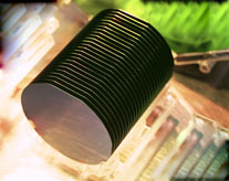
GaSb Wafer (Gallium Antimonide Wafer) »

Product Range
We supply sputtering targets which is manufactured under show unparalleled outstanding performance by virtue of high density, excellent purity, and distinguished homogeneous microstructure. The popular geometries featuring with both planar and rotatable shapes, such as circular, rectangular, ring, tube, cylinder and conicity, are all available. If you have your own unique requirements about the sputtering targets, no matter in density, purity, homogeneity or in geometry, please let us know exactly what you need. We'll do our utmost to meet your requirements precisely.
| 1 | 2",3" GaSb wafer Orientation:(100)±0.5° Thickness(μm):500±25;600±25 Type/Dopant: P/undoped;P/Si;P/Zn Nc(cm-3): (1~2)E17 Mobility(cm2/V ·s):600~700 Growth Method: CZ Polish: SSP |
| 2 | 2" GaSb wafer Orientation:(100)±0.1° Thickness(μm):500±25;600±25 Type/Dopant:N/undoped;P/Te Nc(cm-3): (1~5)E17 Mobility(cm2/V ·s):2500~3500 Growth Method: LEC Polish: SSP |
| 3 | 2" GaSb wafer Orientation:(111)A±0.5° Thickness(μm):500±25 Type/Dopant:N/Te;P/Zn Nc(cm-3):(1~5)E17 Mobility(cm2/V ·s):2500~3500;200~500 Growth Method: LEC Polish: SSP |
| 4 | 2" GaSb wafer Orientation:(111)B±0.5° Thickness(μm):500±25;450±25 Type/Dopant:N/Te;P/Zn Nc(cm-3):(1~5)E17 Mobility(cm2/V ·s):2500~3500;200~500 Growth Method: LEC Polish: SSP |
| 5 | 2" GaSb wafer Orientation: (111)B 2deg.off Thickness(μm): 500±25 Type/Dopant: N/Te;P/Zn Nc(cm-3):(1~5)E17 Mobility(cm2/V ·s):2500~3500;200~500 Growth Method: LEC Polish: SSP |
Note: above wafer specification are standard and we do accordingly customer requirement.
