
Hydrogen Annealed Wafer »
Product Range
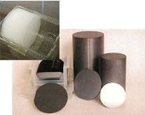
We supply sputtering targets which is manufactured under show unparalleled outstanding performance by virtue of high density, excellent purity, and distinguished homogeneous microstructure. The popular geometries featuring with both planar and rotatable shapes, such as circular, rectangular, ring, tube, cylinder and conicity, are all available. If you have your own unique requirements about the sputtering targets, no matter in density, purity, homogeneity or in geometry, please let us know exactly what you need. We'll do our utmost to meet your requirements precisely.
| Sl. No | Specifications of tender and our confirmation in the below description |
| 1 | Material property Process: CZ |
| 2 | Wafer Type: P-Type |
| 3 | Dopant: Boron |
| 4 | Back Side Damage: No (see back-side surface criteria) |
| 5 | Laser Mark: Hard Marking- (See Fig 3 of attached spec) Backside scribe |
| 6 | Fixed Q.A Diameter: 194 mm with 3 mm off edge Note: The FQA is only applied for SFQR (Site-TIR) and PUA (Site-TIR). |
| 7 | Annealing: Hydrogen annealed Note: The wafers shall be annealed (heat-treated) in an environment of 1200 deg. C, for 1 hour in Hydrogen. |
| 1 | Diameter: 200+/-0.2 mm |
| 2 | Thickness: 725+/-20 micron |
| 3 | Orientation- Notch: (See fig 1 of attached specs) |
| 4 | Bevel Configuration: (See fig 2 of attached specs) |
| 5 | TTV (Parallelism): 4.5 micron (max) |
| 6 | Curvature (Warp): 45 micron (max) |
| 7 | SFQR (TIR – Site): 0.21 micron/22.5 mm sq. (max) Note: Site TIR is front reference. |
| 8 | TIR (PUA) - Site: 100 percent (with 3mm edge exclusion) |
Crystallographic and electrical specifications
| 1 | CRYSTALOGRAPHIC Polished Surface Orientation: 1-0-0 +/- (0.1-1.0 deg) Note:The crystal orientation in the range <1-0-0> - 0.1 deg. to <1-0-0> +0.1 deg. is not allowed. |
| 2 | OSF: 5 Defects/cm2 (max) Note:Heat treatment for OSF and BMD inspections: 780 degC for 3 hr (in dry Oxygen) + 1000 degC for 16 hr (in dry Oxygen). Wafers thermally treated in H2 shall be free from any ring-shaped OSF. |
| 3 | DZ width: 10 micron (min) |
| 4 | BMD & BMD(50): 0.005E09 (min)to 4E09 (max)Counts/cm3 Note: Heat treatment for OSF and BMD inspections: 780 degC for 3 hr (in dry Oxygen) + 1000 degC for 16 hr (in dry Oxygen).Wafers thermally treated in H2 shall be free from any ring-shaped OSF. Measured as per the applicable MPS. |
| 5 |
ELECTRICAL Resistivity: 1.5+/-0.5 ohm-cm |
| 6 | Resistivity Variation: 10 percent (max) |
| 7 | Micro Resistivity Variation: 15 percent (max) |
Impurities & Appearance Specifications Item Specifications –III
| 1 | IMPURITIES Oxygen Concentration (Before H2 annealing) : 13.5E17(min) to 16.5E17 (max) atom/cm3 |
| 2 | Carbon Concentration (Before H2 annealing): 2E16 atom/cm3 (max) |
| 3 | APPEARANCE Surface Impurities (in E10 atoms/cm2) : Na, Al, Ni, Fe, Cr, Cu & Zn = 5 MCL Note: After H2 annealing (without cleaning). |
| 4 | Surface Impurities (in E10 atoms/cm2) : Na, Al, Ni, Fe, Cr, Cu & Zn = 1 MCL Note: After final cleaning |
| 5 | Particles >0.20 micron : 20(max) Counts per wafer |
| 6 | Particles >0.16 micron : 35(max) Counts per wafer |
| 7 | Particles >0.12 micron : 60 (max) Counts per wafer |
| 7 | Particles >0.20 micron : 20(max) Counts per wafer |
| 8 | Front Surface Finishing: Mirror Surface |
| 9 | Back Surface Finishing: Etched surface |
| 10 | Beveled Surface Finishing: Mirror Surface |
| 11 | Chip: 2 (max) Note: 2 chips or less ( 0.8 mm or less in the direction of the circumference and bevel width or less in the direction towards the center). |
| 12 | Spike: 30 (max) per wafer |
Note: above wafer specification are standard and we do accordingly customer requirement.